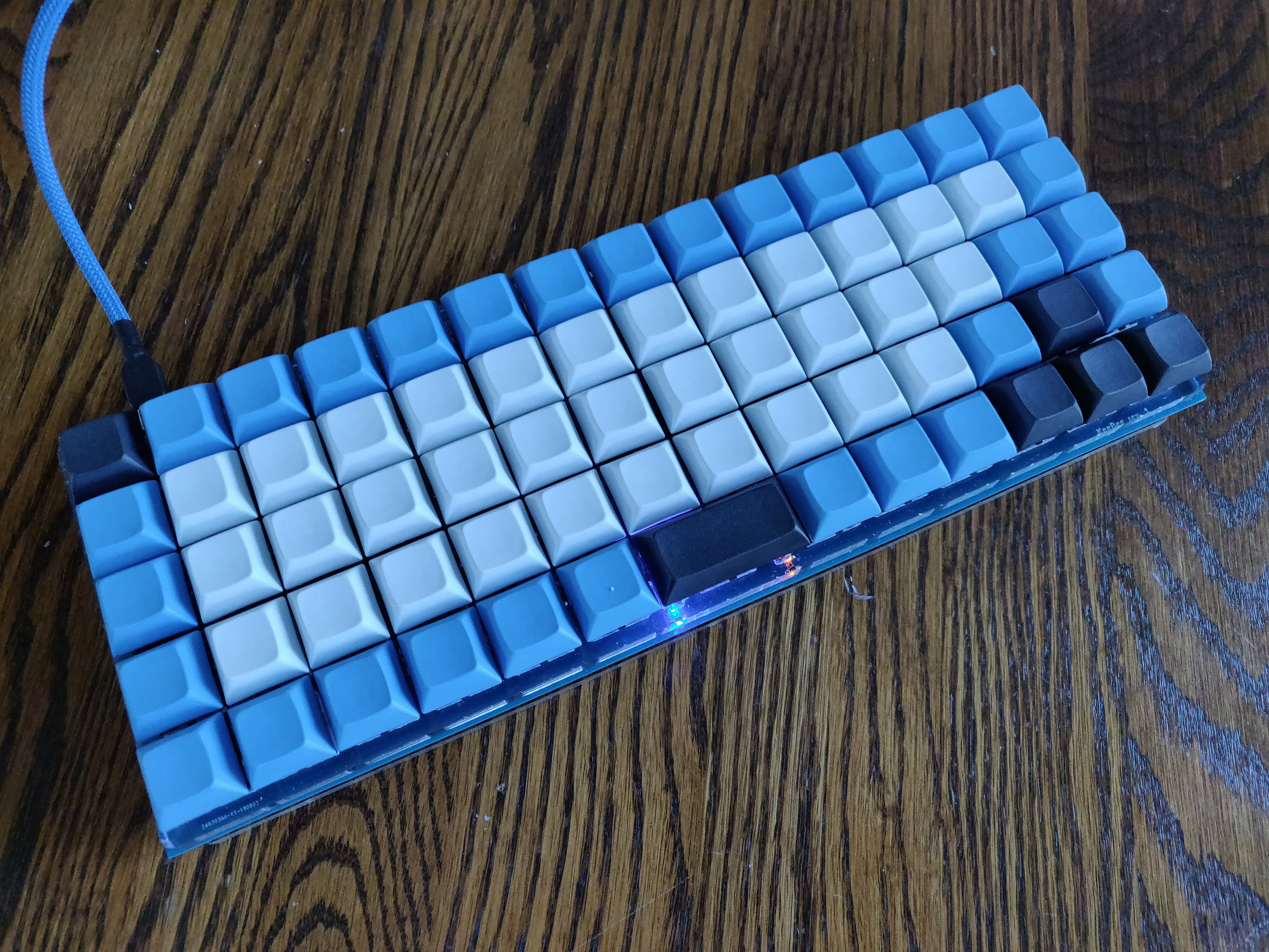
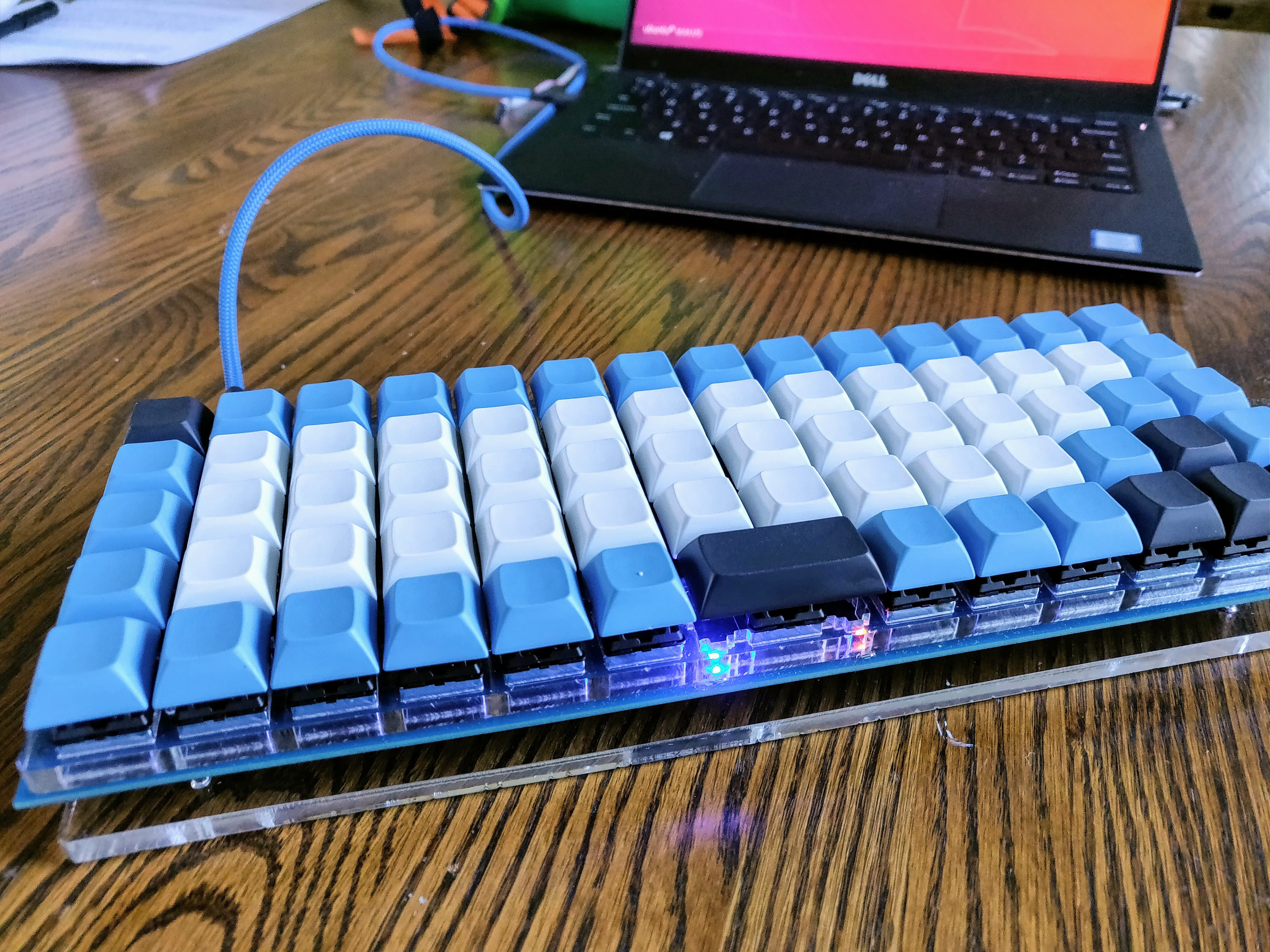
A few months ago, I completed a project to build an entire USB keyboard from scratch. This included electronic circuit design, PCB design, firmware coding, CAD design, assembly and usage. The final result is my daily driver work keyboard, which I affectionately call “KeeBee”:
A few project goals:
- Implement the circuit myself
- Write the keyboard firmware
- Learn about how the USB protocol works
For my day job, I spend most of my time building cloud software that’s many layers removed from real running hardware. It’s extremely safisfying to peel back some of the abstractions, and get closer “to the metal” building real electronic devices I can physically touch and use.
Research & CAD Design
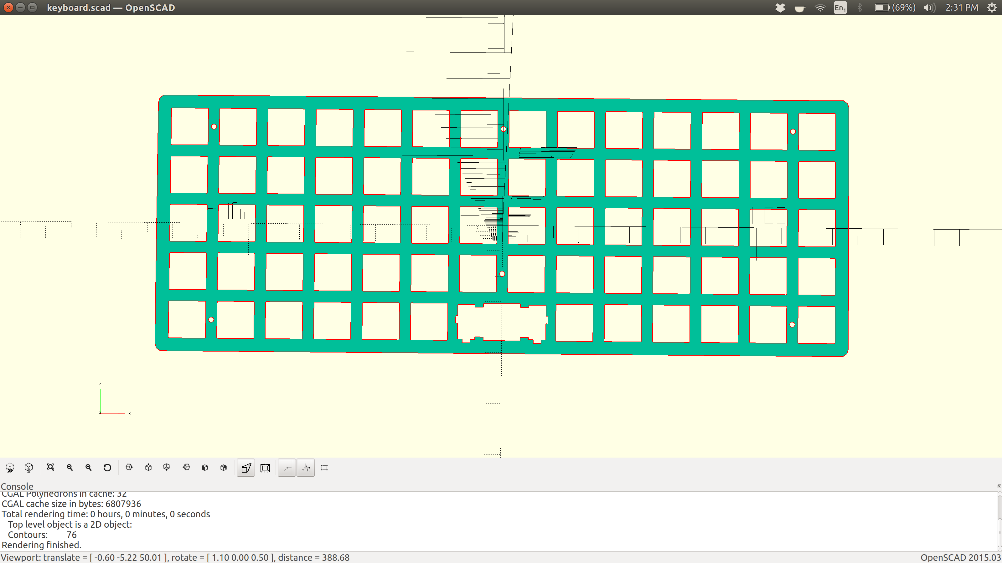
I knew I really liked the OLKB Planck and Preonic style boards. They feature a nice minimal ortho-linear layout, that’s very compact. I also knew that I wanted to use Cherry MX Brown switches. With those two design components in mind, I started playing around with key layouts in OpenSCAD. OpenSCAD is a great open source CAD design tool that functions more like a programming language than a WYSIWYG point and click mouse CAD tool.
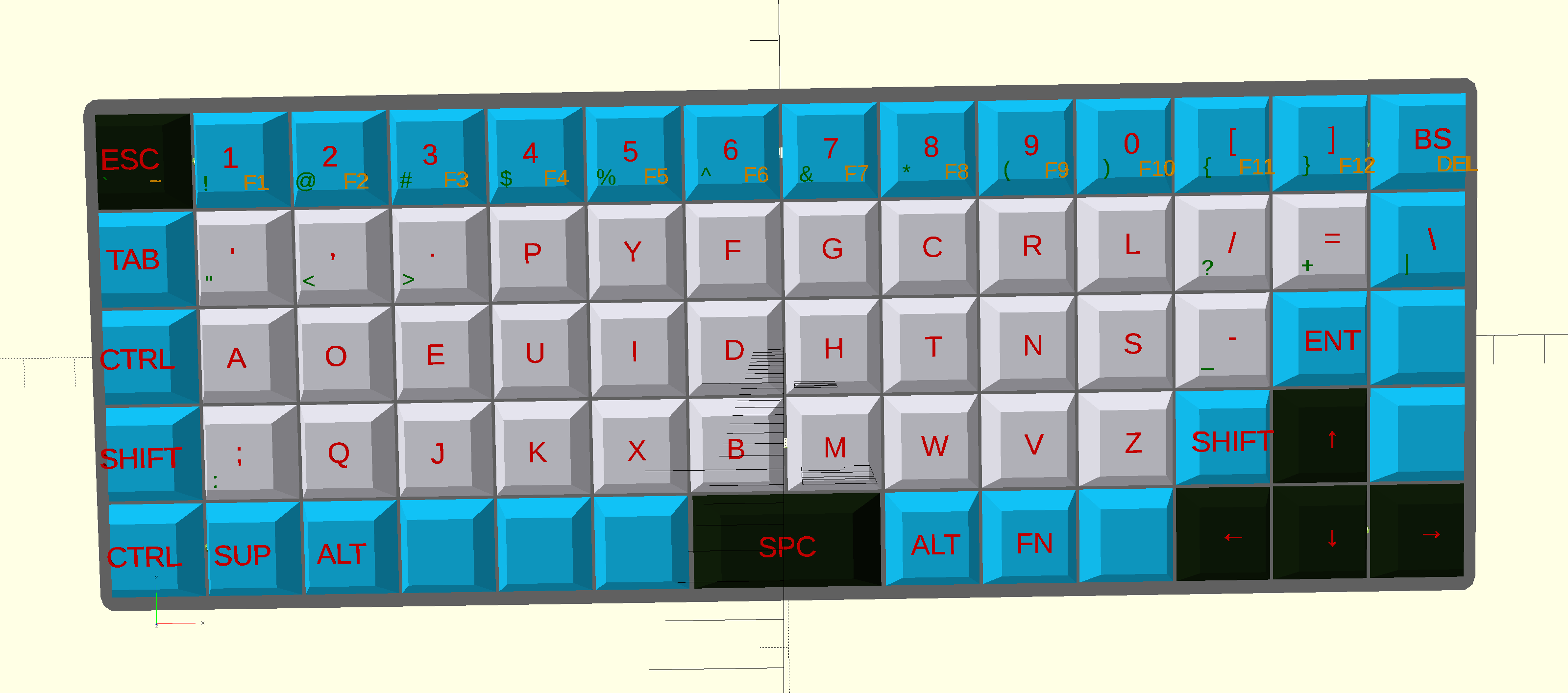
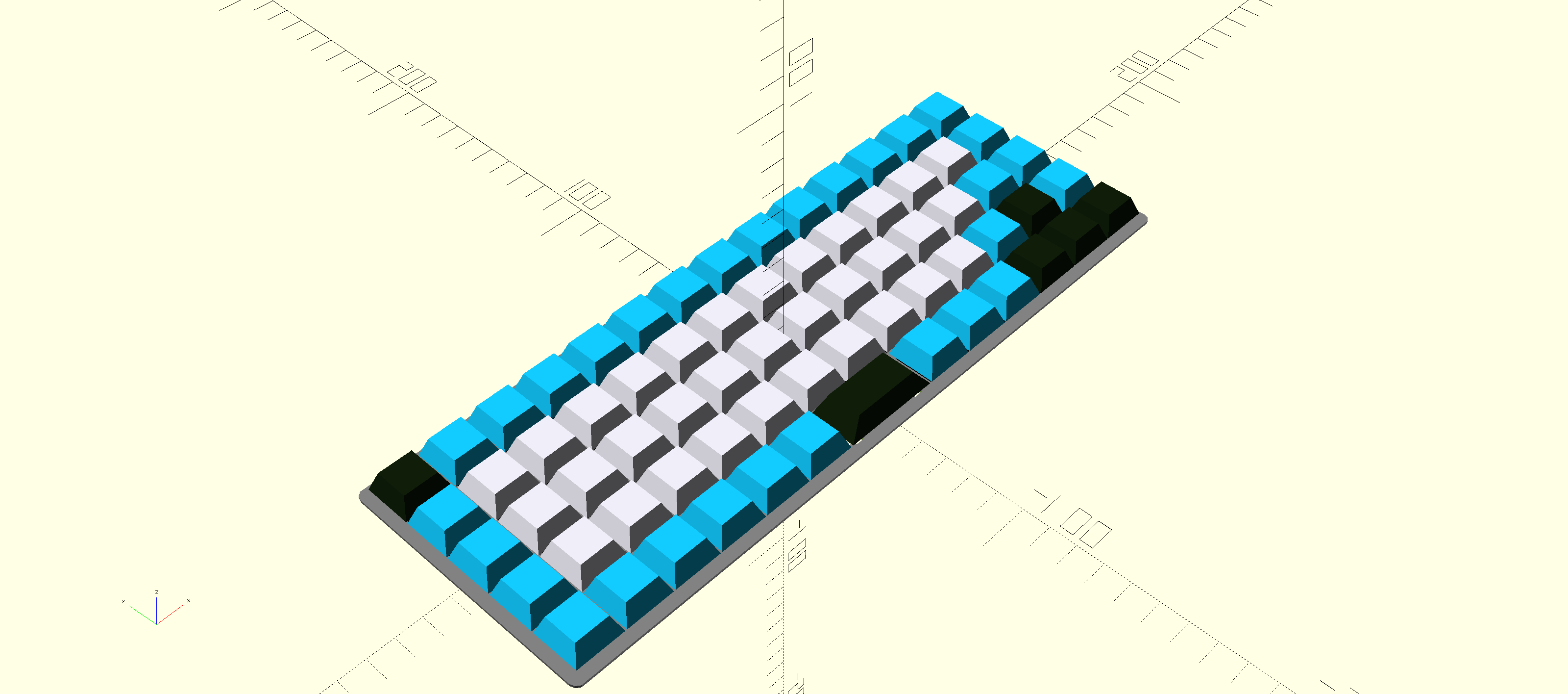
Using the dimensions from a Cherry MX datasheet, I hacked up a keyboard plate design, and then added switches and keycaps to get a feel for what the layout would look like. The top plate sits above the keyboard PCB and serves as a good switch stabilizer.
Top plate design:
With keycaps added:
Prototype Circuit and Firmware Design
I chose an STM32F042K6T6 as the main keyboard microcontroller. It’s around $3 per chip in individual quantities, and has just enough pins to implement a 69 key scan matrix (32 pins in total). It sports an ARM Cortex M0 processor, and has a dedicated USB peripheral for sending out USB bits without tying up the main processor bit-banging out USB signals. I bought a Nucleo prototype development board of this chip for experimenting with the chip before I integrated it into my PCB design. The Nucleo was easy to use on a breadboard, and power directly with USB.
I breadboarded out a small 4 key circuit, to test out the diode based circuit I had researched. Ignoring the USB side of the equation, The first step was to just get the Cherry switches to reliably turn the 4 corresponding LEDs on and off when the button is pressed.

Keyscan Matrix circuits are a technique to use when you have more switches than you have pins on your microcontroller.
After I got the keyscan matrix implementation to my liking, it was time to work on the USB side of the equation.
The inner loop for the firmware is basically:
- Scan all keys in the button keyscan matrix.
- Map the button locations to their respective key symbols, using the currently selected layout (QWERTY, Dvorak, etc.)
- Take the mappings, and generate USB HID Report packets and send them out the USB peripheral.
- Set an LED on the keyboard to on if a key is pressed, off if not.
From main.cc:
static void scan_and_update() {
    scan_matrix.Scan(key_scans, row_count, column_count);
    keyboard.SendReport(
        key_pipeline.MapKeyScans(key_scans, key_count));
    update_key_press_status();
}

int main() {
    Init();

    status_led.SetOk(true);
    while (true) {
        scan_and_update();
    }
}
The keyboard.SendReport component is the piece that actually sends
the USB packets to the host. I struggled a lot to get USB working
correctly. There are a lot of finnicky layers to the USB protocol that require
accurate timing,
and correct device identification. I
ended up needing to fire up Wireshark to sniff USB packets coming back
and forth to my Linux laptop, in order to debug where things were getting
lost on the wire. Most of my googling was pretty useless at this part of the
build: suggestions I found had suggestions like, “You probably have a
faulty USB device, you should get a new one.” When you’re the one actually trying to
build the USB device, this isn’t really helpful. I was left reading through very large USB
specifications that contain a lot of terminology that was pretty
unfamiliar to me.
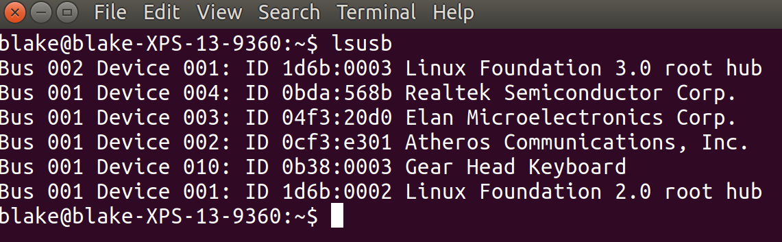
After mucking about for awhile, I was able to get the 4 key keyboard to correctly identify itself as a USB HID (Human Interface Device) to my laptop, and make sure all my key presses were being correctly mapped to the machine:
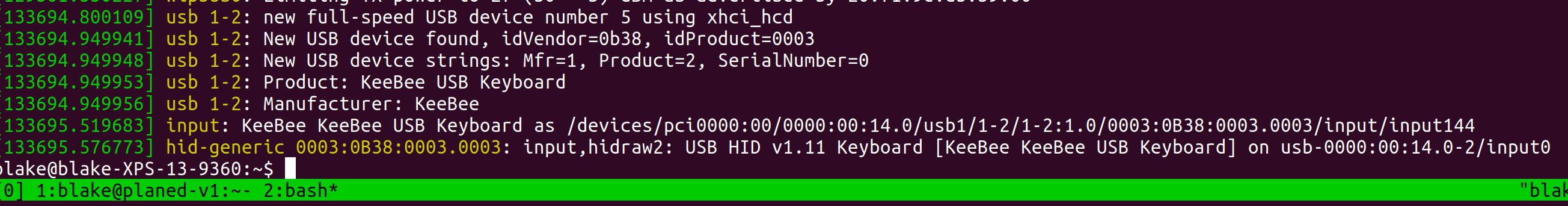
Getting a USB vendor and device id requires paying a good bit of cash, so if you’re just doing something as a hobby, you’ll need to hijack a similar device ID. I thought “Gear Head” sounded cool, and they make a keyboard, so I went with that one.
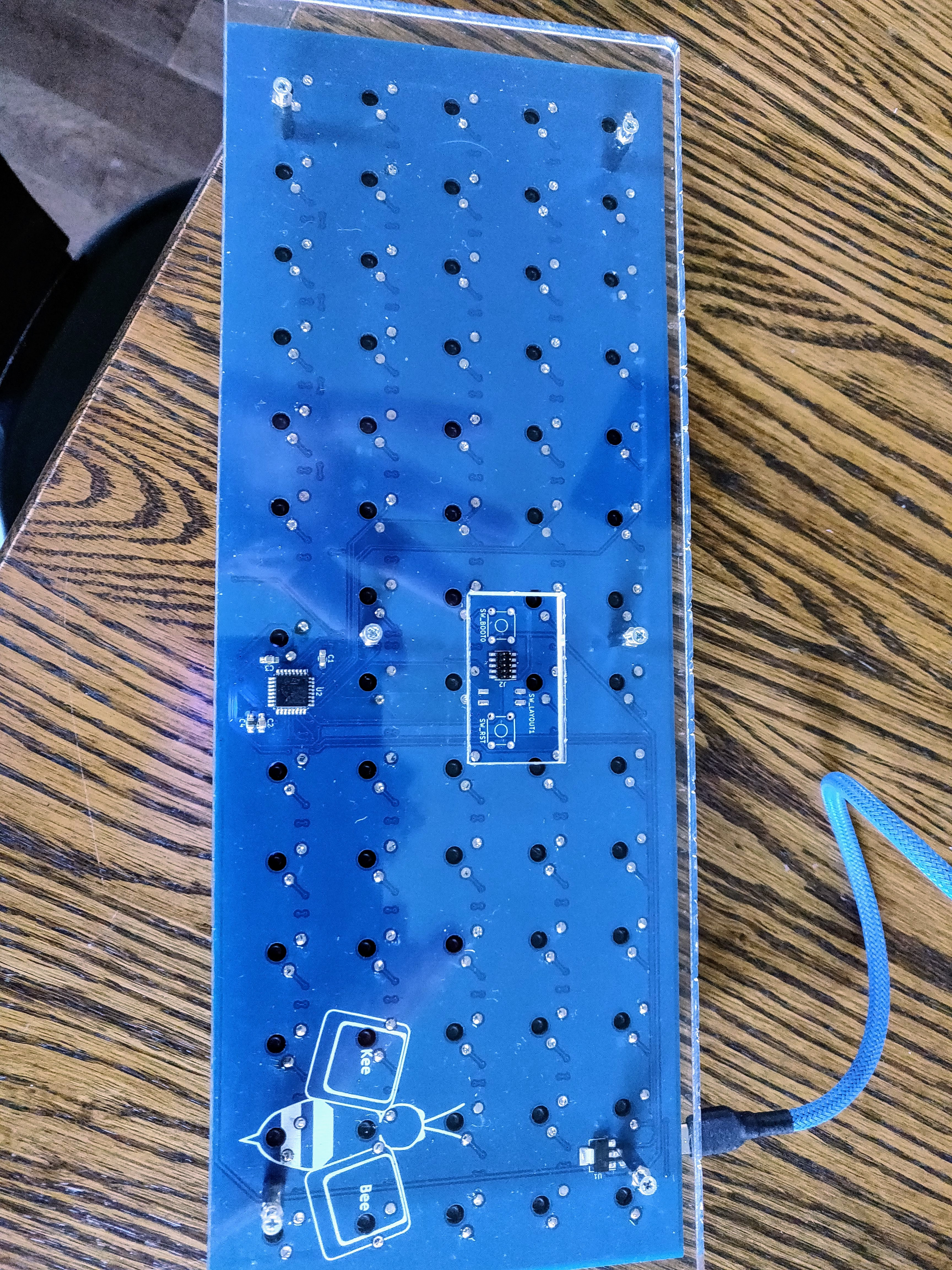
Schematic and PCB Design
With some working firmware on a working prototype, it’s time to put the schematic and PCB design into KiCAD and get an actual printed circuit board made. Now that I had proven the schematic design worked, it was relatively straight-forward to connect everything together schematic wise:

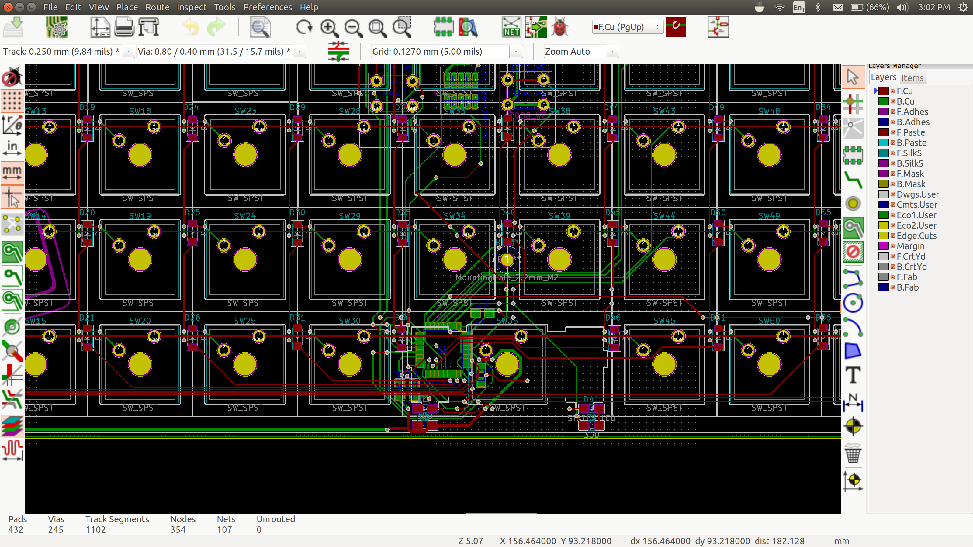
After building out the schematic and selecting part footprints, we need to layout the actual physical PCB:
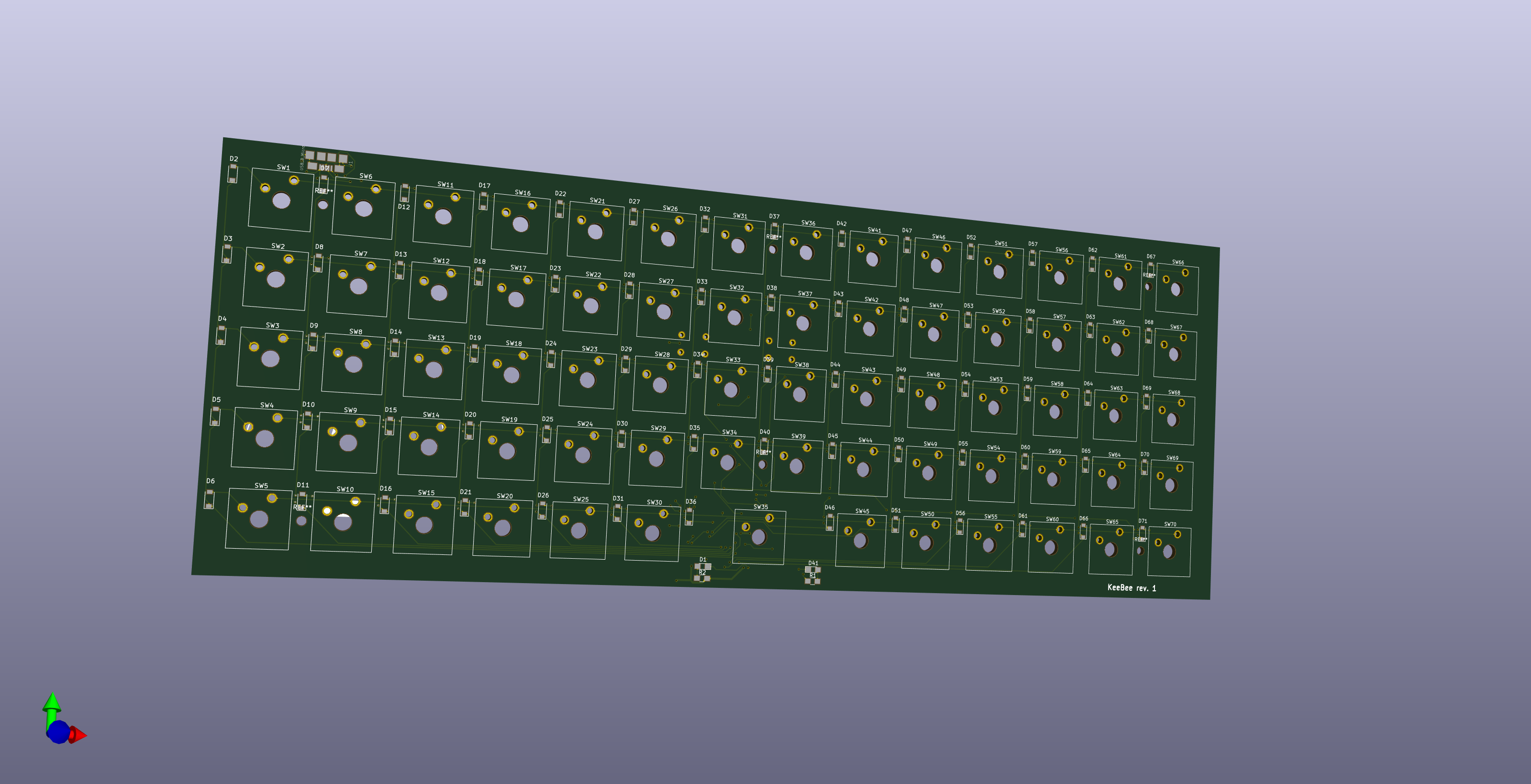
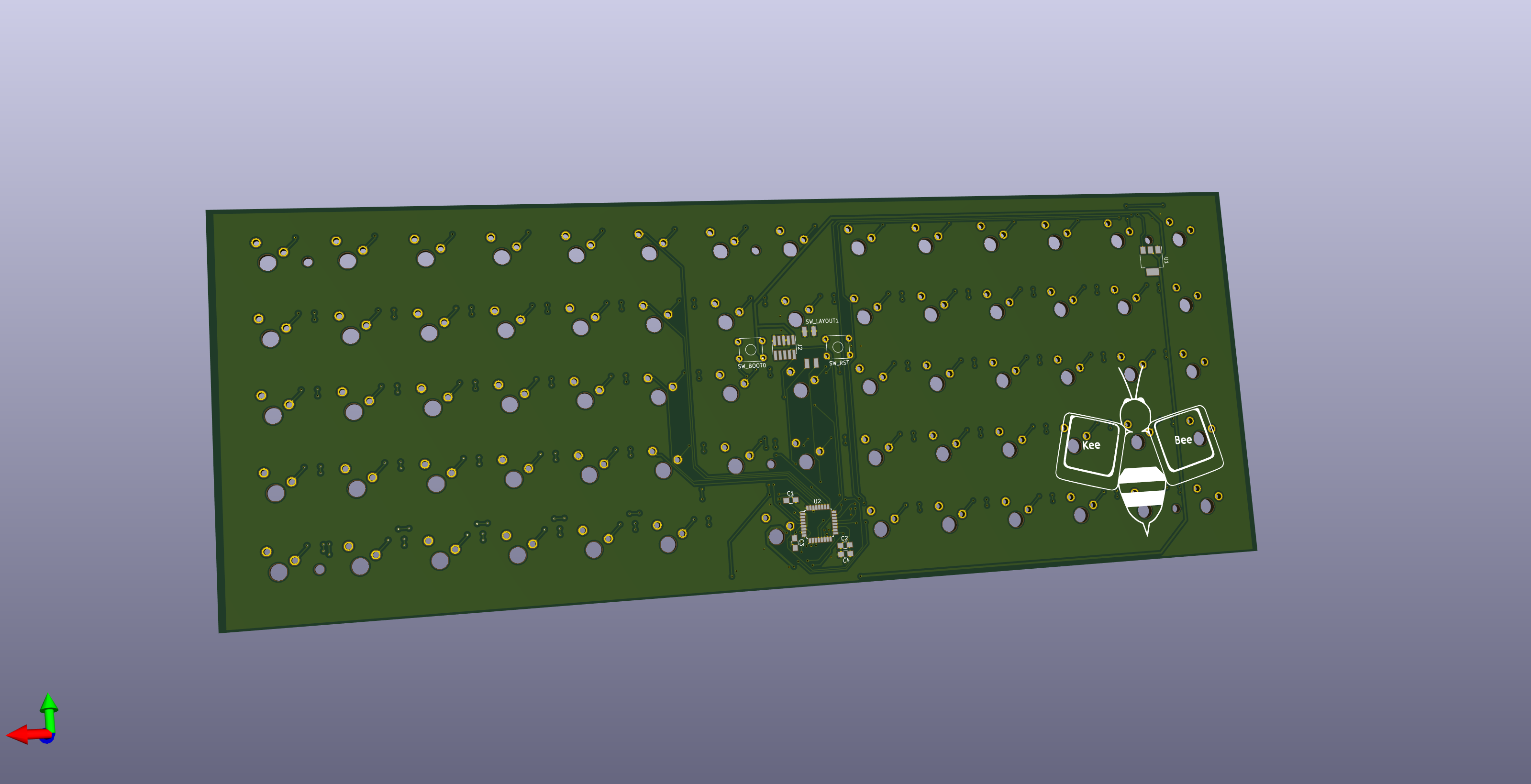
KiCAD has a neat feature that lets you preview your PCB in 3D:
There are lots of great tutorials on how to use KiCAD. I started with Chris Gammell’s excellent Getting to Blinkey 4.0 youtube series, where he takes you through building a LED blinker PCB circuit in KiCAD from start to finish.
PCB and Component Ordering
Once I was reasonably satisfied with the schematic and PCB design, I started placing a bunch of orders:
- All the board components from the keyboard’s Bill of Materials: Switches, LEDs, diodes, microcontrollers, etc. I like to use DigiKey for most of my electronic components.
- The PCB itself. There are a lot of really great PCB prototype manufacturing services out there that will do small run PCB fabrication for really cheap. I’ve had great experience with OshPark and JLCPCB. For this project, I went with JLCPCB because of the board size cost, and because they let me pick a blue solder-mask board.
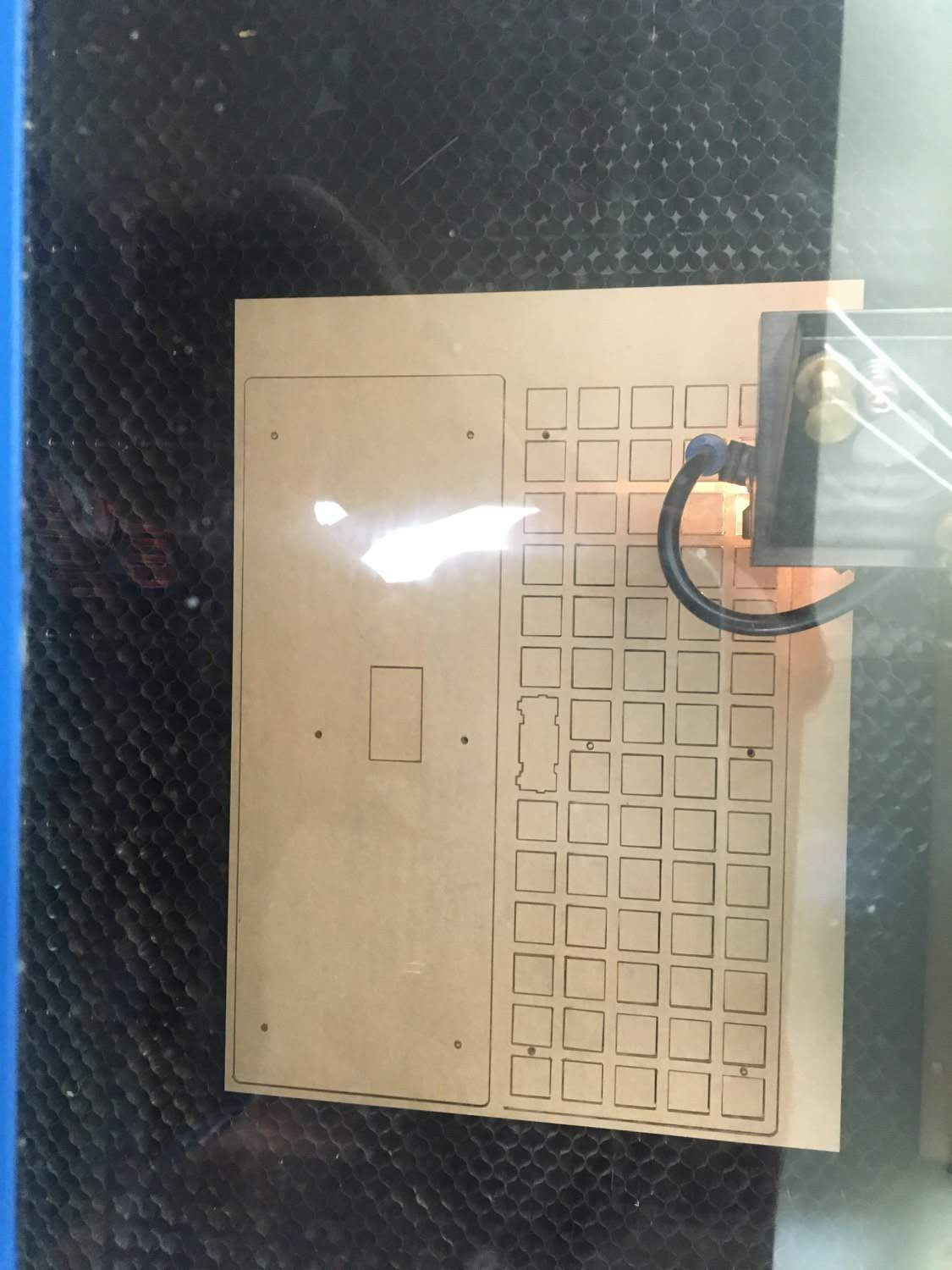
- Any other cases, etc. For this project, my brother in law was able to laser cut the top and bottom keyboard plates from 1/4” acryllic sheets. There are other great online laser cutting and 3D printing services for case components, if you don’t have access to the equipment.
PCB arrival day is the the best:
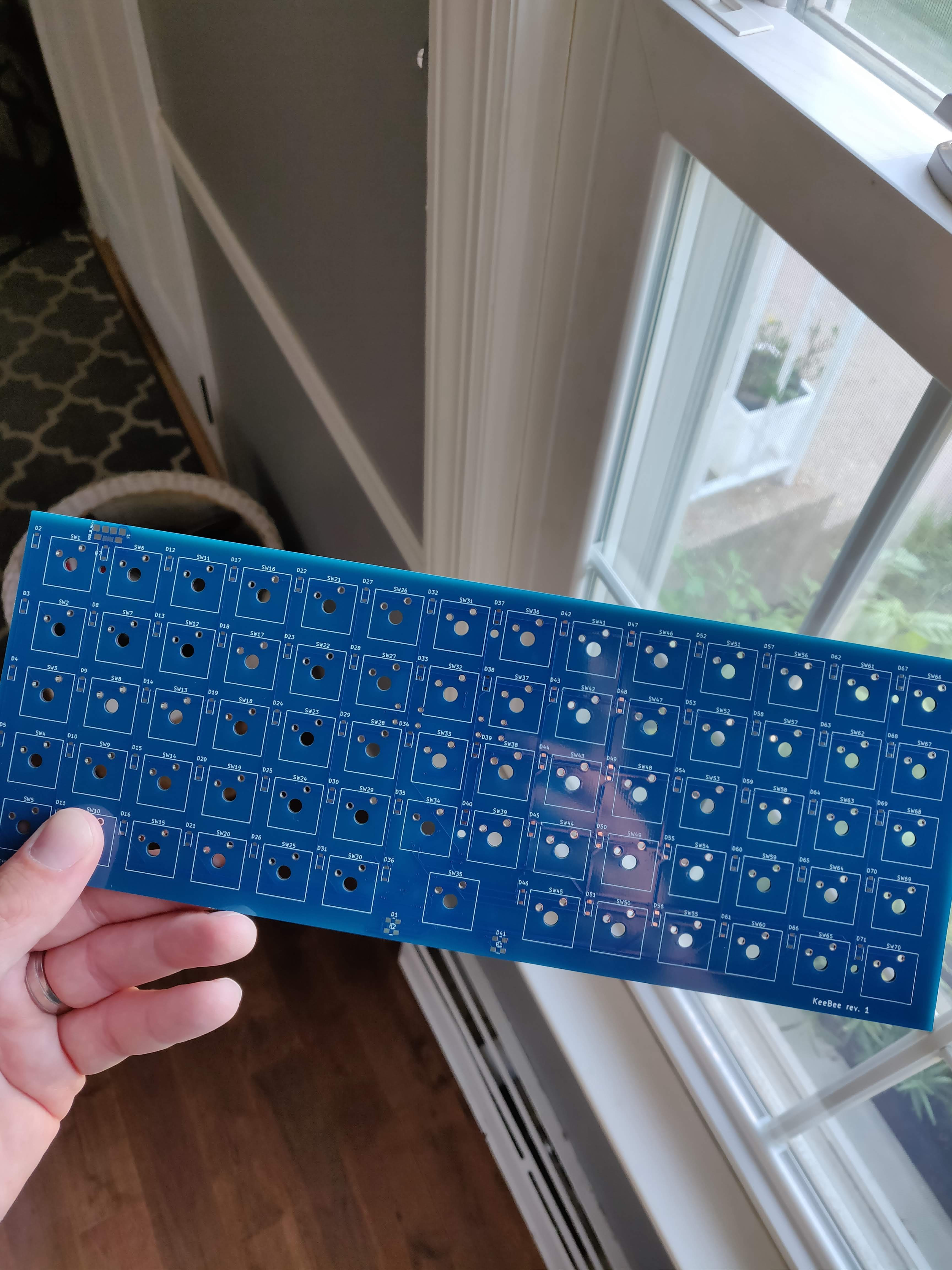
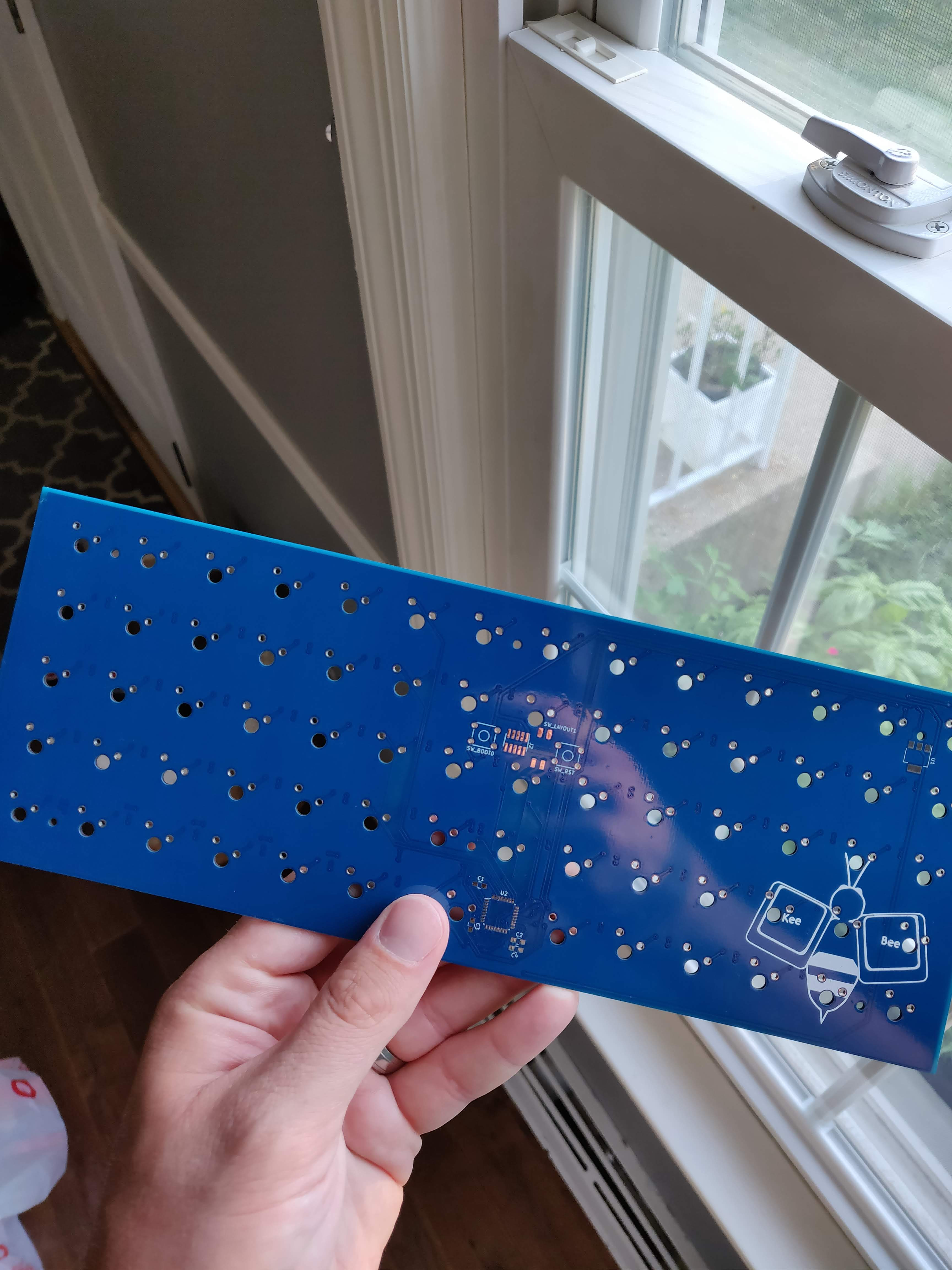
JLCPCB is very affordable. This design was less than $30 shipped DHL from China, and took a little over a week to arrive after submitting my gerber files for order.
My brother in law took my DXF files from OpenSCAD and tossed them in the laser cutter:
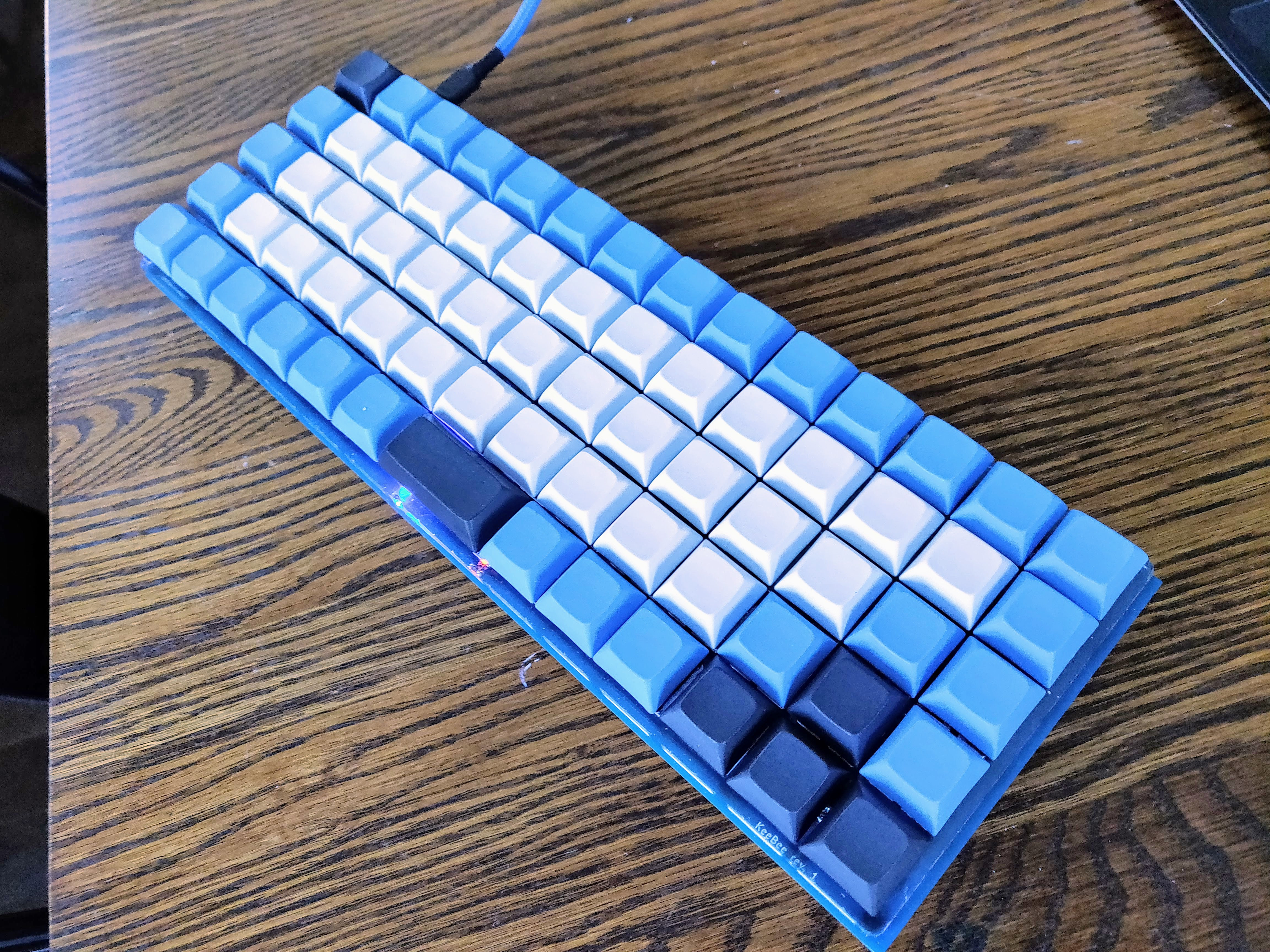
Final Assembly
With all the pieces ordered and fabricated, it was time to put the final keyboard together. I started with PCB component assembly: I used a soldering iron for the larger electronic components and a hot air rework station for the small surface mount components like the STM32 microcontroller.
Total component build time for a board was roughly 3 hours - most of the time was spent soldering the 70 diodes and switches.
I added a JTAG debugger pin header to the PCB, which I used to plug in a JLINK Edu mini to flash the microcontroller with the firmware with OpenOCD.
From there, it was final testing, and plate assembly:
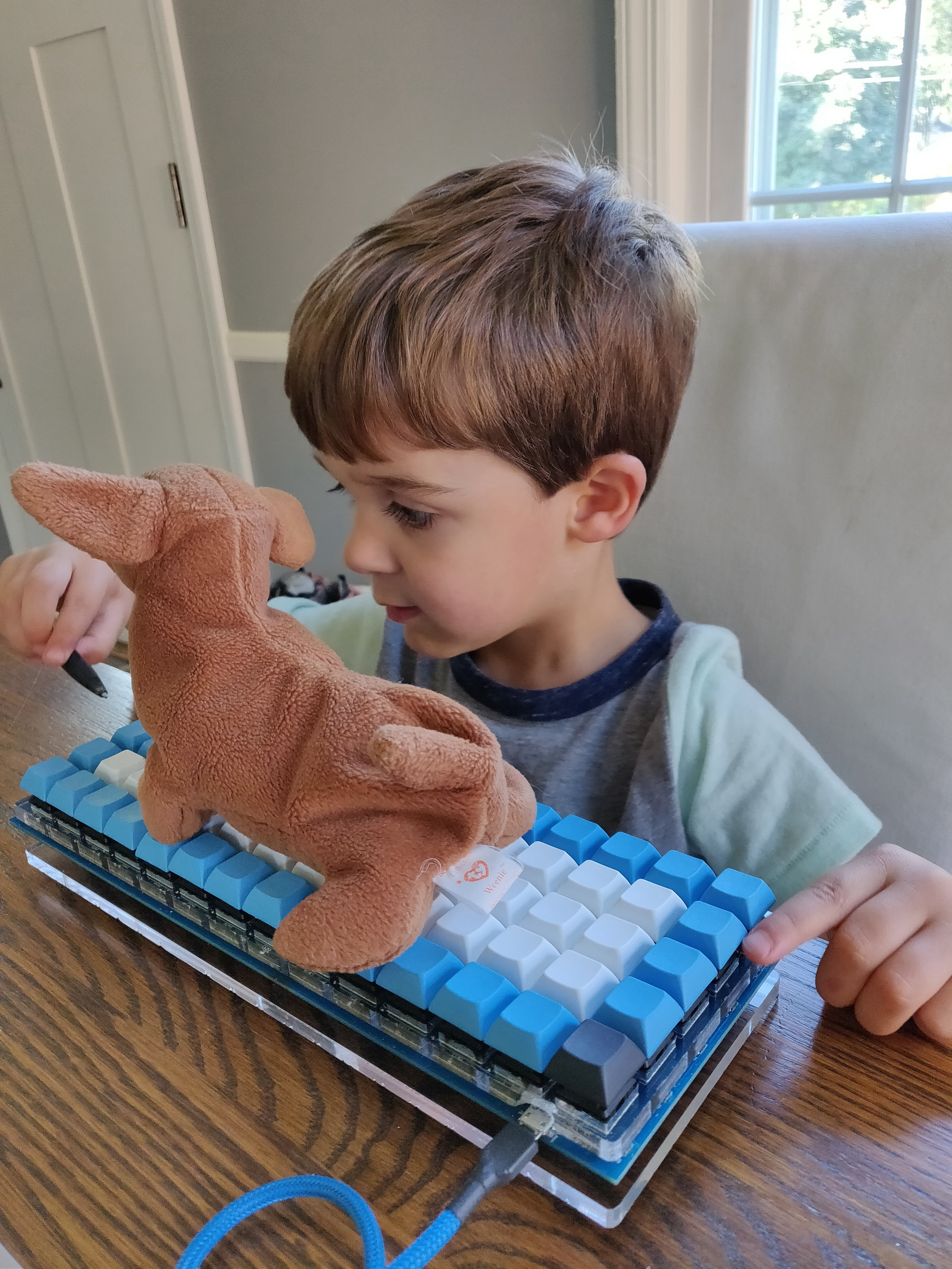
My son thought it made a great train for his animals:

Conclusion
From initial idea to final assembly, this project took about 3 months time. It was extremely rewarding to make something that I still use everyday at work.
All the project files are up on GitHub, including firmware source code, PCB schematics, Bill of Materials, and CAD models.
Thanks for reading, and happy hardware hacking!